The board schematics and the choice of chip set are an important step when developing an electronic product. Let’s look into this, in this third article in our series (part 1 is here, part 2 is here)
In a complex product system like we are discussing with the drone intruder interceptor, there will be multiple printed circuit board assemblies (PCBA), each having a specific function within the system.
- Some of these PCBAs will be size sensitive, which may require dedicated miniature or micro components (that brings its own set of challenges while designing the PCB).
- Other PCBAs will be less sensitive to size but will need careful design consideration when it comes to power management, whereas some of the PCBA will have multiple functions designed into them (e.g. wifi and other communication devices as well as power distribution and safety features to protect the main device and its control systems).
Do you need to understand all this?
If you have an overall understanding of the process and if you work with an engineer specializing in this field, you can maximize the chances that your product will get to production faster (fewer prototyping iterations) and will perform as expected.
What many companies do is find a Chinese contract manufacturer that will do all the development. This is typical of hardware startups that have raised money through Kickstarter, Indigogo, or traditional investors. But do you want to rely on them entirely? Do you want, 18 months down the road, to beg them to make that tiny little change for a reasonable cost?
Note that there is a good case to be made, in many situations, for the buyer to pay a service provider to do the development and then a manufacturer just for manufacturing. You will avoid risks of IP appropriation.
What is the overall logic to follow to design a PCBA schematic?
There is a logical process that should be followed (shown in the diagram below) when designing a PCB and best practice guidelines which should be followed in order to design a quality and reliable PCB.
Each PCB starts with ‘what is needed’ from a functionality aspect. It will drive the design, including component types and overall dimensions.
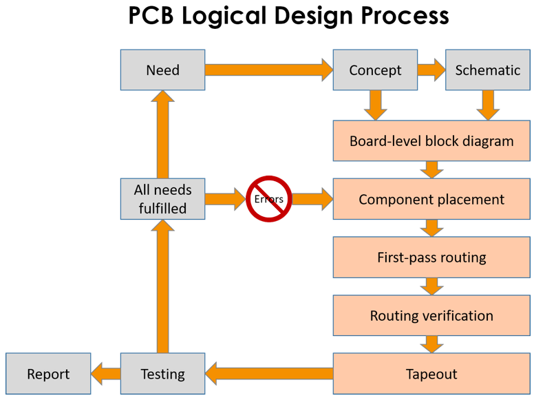
Once the initial concept for each PCB has been generated, the next step is to create schematic diagrams for each of the boards. This is what is covered in this article.
General guidelines for designing a schematic diagram
A schematic diagram is a representation of the PCB design using symbols to show components, tracks, connections and other important information about the actual design. (The layout of a PCB schematic diagram may not necessarily correspond to the physical arrangement of the finished product.)
There are a set of guidelines that should be followed when generating your PCB schematic diagrams. You need to ensure your design team (or your supplier if they take care of this part of the design) follows these guidelines, which include the following:
1. Use common designators
The use of standardized symbols provides a common understanding when it comes to reading the schematic, as the objective of any schematic diagram is to transfer information from the designer to the manufacturer.
2. Text placement
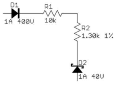
Placing the text which identifies the name and value of each component or connection is just as important to get right as the layout itself. Making sure the text is correctly orientated and close enough to the component symbol it is associated with is key to creating a clear and concise drawing. Here is a good example of correct text placement:
3. Basic layout & flow
As a rule of thumb, it is best to have higher voltages placed towards the top, lower voltages placed towards the bottom and a logical flow from left to right. This way it is easy for the reader to understand the schematic layout.
4. IC Pin layout
Show pins of ICs in position relevant to their function (not how they happen to stick out of the chip). Try to put positive power pins at top, negative power pins (usually grounds) at bottom, inputs at left, and outputs at right.
Note that this fits with the general schematic layout as described above in basic layout & flow. This isn’t always reasonable and possible, but general-purpose parts like microcontrollers and FPGAs have pins that can be input and output depending on use. At least you can put the dedicated power and ground pins at top and bottom, and possibly group together any closely related pins with dedicated functions, like crystal driver connections.
It is a lot easier for the engineer to analyze something with a scope when the pin is related to a specific function as opposed to working out what each pin is. An example of this would for the engineer to ask the question, “I need to check the clock speed, what pin is that?” and NOT “I need to look at pin number 8, what function is that?”.
5. Drawing size format
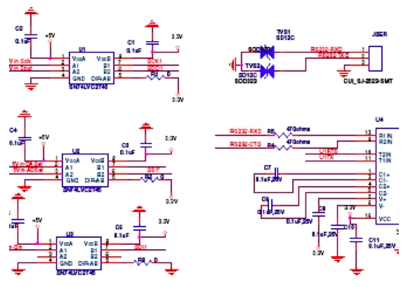
Something as simple as the page layout will help those reading the schematic understand it better. If your schematic is large, which it most likely would be for the drone project, cramming everything onto a single page just makes it difficult to read on both a computer and as a print out.
It is best to use more pages as it is easier to flip pages by hand or skip to the next page at a click of a button as opposed to zooming in and panning around or trying to find a plotter in-order to print out an oversized sheet of paper. It is also better to break up the schematic into sections and have one part of the schematic per page.
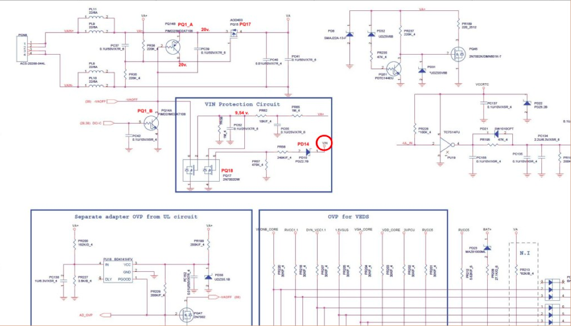
Here is an example of where that would work nicely:
6. Naming Convention
Most schematic software programs will allow you manually name items and often allow 32 to 64 characters but it is best to keep the naming convention as short as possible.
The key point is clarity in the information you are putting across and long names just congests the page with text. An example of a shortened text would be from “8MHz clock” to “CLK”. When it comes to IC Pin abbreviations there is an ANSI/IEEE standard that should be followed.
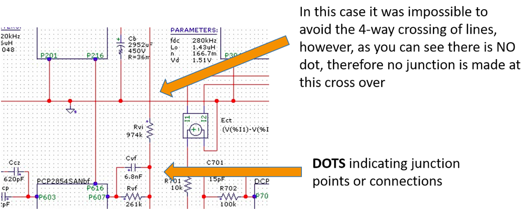
7. Dots and Crosses
The rule here is to draw a DOT at every junction and to always keep junctions to Ts and not 4-way crosses. If lines do cross at 90 degrees they are never connected as a junction point, this way it keeps the schematic clear and easy to understand. When there is a junction, ALWAYS include the dot to indicate junction point.
The diagram below shows an example of dots as well as an unavoidable 4-way cross:
Some of the standard symbols that are used in PCB schematic diagrams are shown in the image below:
Source for some of this information: Stack Exchange.
The purpose of this series is not to give you the skills to develop a new electronic product, but to help you understand what it takes. All this can be very well done or very poorly done.
In other words, don’t work with a low-cost design team, and don’t count on a Chinese factory that only has a junior electrical engineer (who knows where they will subcontract the work).
No comments:
Post a Comment